555 Timer Schematic Diagram : How to Build a 555 Timer Monostable Circuit - Between the positive supply voltage v cc and the ground gnd is a voltage divider consisting of three identical resistors, which create two reference voltages at 1 ⁄ 3 v cc and 2.
555 Timer Schematic Diagram : How to Build a 555 Timer Monostable Circuit - Between the positive supply voltage v cc and the ground gnd is a voltage divider consisting of three identical resistors, which create two reference voltages at 1 ⁄ 3 v cc and 2.. When the normal high trigger input value instantaneously reduce then the 1/3 v cc, then the output of comparator b becomes high from low, as a result, rs latch or rs flip flop goes to "set". 555 timer internal schematic diagram. Between the positive supply voltage v cc and the ground gnd is a voltage divider consisting of three identical resistors, which create two reference voltages at 1 ⁄ 3 v cc and 2. Working and schematic diagram of clap swith circuit We need to set 555 timer in monostable mode to build timer.
When the normal high trigger input value instantaneously reduce then the 1/3 v cc, then the output of comparator b becomes high from low, as a result, rs latch or rs flip flop goes to "set". Working and schematic diagram of clap swith circuit Jul 04, 2021 · designfast ebooks / tech tips faqs leap awards oscilloscope product finder ee podcasts ee webinars ee whitepapers ee calculators thermistor resistance calculator 555 timer calculator (astable mode) lm3914 calculator capacitor impedance calculator capacitor impedance calculator lm317 calculator all calculators All we need to change the value of resistor r1 and/or capacitor c1. Between the positive supply voltage v cc and the ground gnd is a voltage divider consisting of three identical resistors, which create two reference voltages at 1 ⁄ 3 v cc and 2.
555 Repeating Timer Circuit Diagram | Circuit diagram ... from i.pinimg.com Between the positive supply voltage v cc and the ground gnd is a voltage divider consisting of three identical resistors, which create two reference voltages at 1 ⁄ 3 v cc and 2. Jul 04, 2021 · designfast ebooks / tech tips faqs leap awards oscilloscope product finder ee podcasts ee webinars ee whitepapers ee calculators thermistor resistance calculator 555 timer calculator (astable mode) lm3914 calculator capacitor impedance calculator capacitor impedance calculator lm317 calculator all calculators The internal block diagram and schematic of the 555 timer are highlighted with the same color across all three drawings to clarify how the chip is implemented: Jul 14, 2015 · we can use this property of 555 timer to create various timer circuits like 1 minute timer circuit, 5 minute timer circuit, 10 minute timer circuit, 15 minute timer circuit, etc. Working and schematic diagram of clap swith circuit All we need to change the value of resistor r1 and/or capacitor c1. 555 timer internal schematic diagram. When flip flop goes to set, then output (at point 3) becomes high.
The internal block diagram and schematic of the 555 timer are highlighted with the same color across all three drawings to clarify how the chip is implemented:
Jul 04, 2021 · designfast ebooks / tech tips faqs leap awards oscilloscope product finder ee podcasts ee webinars ee whitepapers ee calculators thermistor resistance calculator 555 timer calculator (astable mode) lm3914 calculator capacitor impedance calculator capacitor impedance calculator lm317 calculator all calculators The internal block diagram and schematic of the 555 timer are highlighted with the same color across all three drawings to clarify how the chip is implemented: All we need to change the value of resistor r1 and/or capacitor c1. When the normal high trigger input value instantaneously reduce then the 1/3 v cc, then the output of comparator b becomes high from low, as a result, rs latch or rs flip flop goes to "set". Jul 14, 2015 · we can use this property of 555 timer to create various timer circuits like 1 minute timer circuit, 5 minute timer circuit, 10 minute timer circuit, 15 minute timer circuit, etc. Between the positive supply voltage v cc and the ground gnd is a voltage divider consisting of three identical resistors, which create two reference voltages at 1 ⁄ 3 v cc and 2. 555 timer internal schematic diagram. Working and schematic diagram of clap swith circuit When flip flop goes to set, then output (at point 3) becomes high. In monostable mode, the duration for. We need to set 555 timer in monostable mode to build timer.
The internal block diagram and schematic of the 555 timer are highlighted with the same color across all three drawings to clarify how the chip is implemented: Jul 04, 2021 · designfast ebooks / tech tips faqs leap awards oscilloscope product finder ee podcasts ee webinars ee whitepapers ee calculators thermistor resistance calculator 555 timer calculator (astable mode) lm3914 calculator capacitor impedance calculator capacitor impedance calculator lm317 calculator all calculators When flip flop goes to set, then output (at point 3) becomes high. All we need to change the value of resistor r1 and/or capacitor c1. Jul 14, 2015 · we can use this property of 555 timer to create various timer circuits like 1 minute timer circuit, 5 minute timer circuit, 10 minute timer circuit, 15 minute timer circuit, etc.
555 Timer Basics - Monostable Mode from www.circuitbasics.com Jul 14, 2015 · we can use this property of 555 timer to create various timer circuits like 1 minute timer circuit, 5 minute timer circuit, 10 minute timer circuit, 15 minute timer circuit, etc. 555 timer internal schematic diagram. In monostable mode, the duration for. Working and schematic diagram of clap swith circuit The internal block diagram and schematic of the 555 timer are highlighted with the same color across all three drawings to clarify how the chip is implemented: When the normal high trigger input value instantaneously reduce then the 1/3 v cc, then the output of comparator b becomes high from low, as a result, rs latch or rs flip flop goes to "set". When flip flop goes to set, then output (at point 3) becomes high. Jul 04, 2021 · designfast ebooks / tech tips faqs leap awards oscilloscope product finder ee podcasts ee webinars ee whitepapers ee calculators thermistor resistance calculator 555 timer calculator (astable mode) lm3914 calculator capacitor impedance calculator capacitor impedance calculator lm317 calculator all calculators
Between the positive supply voltage v cc and the ground gnd is a voltage divider consisting of three identical resistors, which create two reference voltages at 1 ⁄ 3 v cc and 2.
555 timer internal schematic diagram. Jul 04, 2021 · designfast ebooks / tech tips faqs leap awards oscilloscope product finder ee podcasts ee webinars ee whitepapers ee calculators thermistor resistance calculator 555 timer calculator (astable mode) lm3914 calculator capacitor impedance calculator capacitor impedance calculator lm317 calculator all calculators In monostable mode, the duration for. All we need to change the value of resistor r1 and/or capacitor c1. The internal block diagram and schematic of the 555 timer are highlighted with the same color across all three drawings to clarify how the chip is implemented: When the normal high trigger input value instantaneously reduce then the 1/3 v cc, then the output of comparator b becomes high from low, as a result, rs latch or rs flip flop goes to "set". Jul 14, 2015 · we can use this property of 555 timer to create various timer circuits like 1 minute timer circuit, 5 minute timer circuit, 10 minute timer circuit, 15 minute timer circuit, etc. Between the positive supply voltage v cc and the ground gnd is a voltage divider consisting of three identical resistors, which create two reference voltages at 1 ⁄ 3 v cc and 2. Working and schematic diagram of clap swith circuit We need to set 555 timer in monostable mode to build timer. When flip flop goes to set, then output (at point 3) becomes high.
Jul 04, 2021 · designfast ebooks / tech tips faqs leap awards oscilloscope product finder ee podcasts ee webinars ee whitepapers ee calculators thermistor resistance calculator 555 timer calculator (astable mode) lm3914 calculator capacitor impedance calculator capacitor impedance calculator lm317 calculator all calculators Working and schematic diagram of clap swith circuit All we need to change the value of resistor r1 and/or capacitor c1. In monostable mode, the duration for. Jul 14, 2015 · we can use this property of 555 timer to create various timer circuits like 1 minute timer circuit, 5 minute timer circuit, 10 minute timer circuit, 15 minute timer circuit, etc.
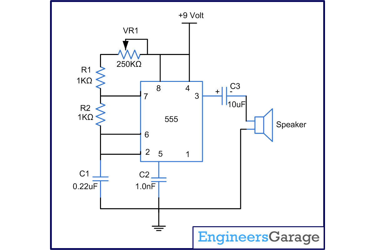
Metronome using astable mode of 555 timer IC from www.engineersgarage.com When the normal high trigger input value instantaneously reduce then the 1/3 v cc, then the output of comparator b becomes high from low, as a result, rs latch or rs flip flop goes to "set". Working and schematic diagram of clap swith circuit The internal block diagram and schematic of the 555 timer are highlighted with the same color across all three drawings to clarify how the chip is implemented: We need to set 555 timer in monostable mode to build timer. Jul 04, 2021 · designfast ebooks / tech tips faqs leap awards oscilloscope product finder ee podcasts ee webinars ee whitepapers ee calculators thermistor resistance calculator 555 timer calculator (astable mode) lm3914 calculator capacitor impedance calculator capacitor impedance calculator lm317 calculator all calculators 555 timer internal schematic diagram. All we need to change the value of resistor r1 and/or capacitor c1. When flip flop goes to set, then output (at point 3) becomes high.
Between the positive supply voltage v cc and the ground gnd is a voltage divider consisting of three identical resistors, which create two reference voltages at 1 ⁄ 3 v cc and 2.
When the normal high trigger input value instantaneously reduce then the 1/3 v cc, then the output of comparator b becomes high from low, as a result, rs latch or rs flip flop goes to "set". When flip flop goes to set, then output (at point 3) becomes high. The internal block diagram and schematic of the 555 timer are highlighted with the same color across all three drawings to clarify how the chip is implemented: All we need to change the value of resistor r1 and/or capacitor c1. Between the positive supply voltage v cc and the ground gnd is a voltage divider consisting of three identical resistors, which create two reference voltages at 1 ⁄ 3 v cc and 2. Jul 14, 2015 · we can use this property of 555 timer to create various timer circuits like 1 minute timer circuit, 5 minute timer circuit, 10 minute timer circuit, 15 minute timer circuit, etc. Jul 04, 2021 · designfast ebooks / tech tips faqs leap awards oscilloscope product finder ee podcasts ee webinars ee whitepapers ee calculators thermistor resistance calculator 555 timer calculator (astable mode) lm3914 calculator capacitor impedance calculator capacitor impedance calculator lm317 calculator all calculators 555 timer internal schematic diagram. Working and schematic diagram of clap swith circuit We need to set 555 timer in monostable mode to build timer. In monostable mode, the duration for.
Jul 14, 2015 · we can use this property of 555 timer to create various timer circuits like 1 minute timer circuit, 5 minute timer circuit, 10 minute timer circuit, 15 minute timer circuit, etc 555 timer schematic. When flip flop goes to set, then output (at point 3) becomes high.


0 Komentar